FET circuit design
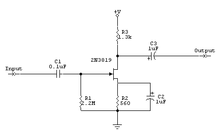 This circuit
originates
from the famous RS-4 INSPIRE VLF receiver. It
is actually a modified version of it. The modification
increased the gain a little bit. Care must be taken
when connecting the FET to the circuit- be sure the
leads are in thier proper places. The source lead connects to
the grounded side of the circuit (R2). The drain
lead connects to the V+ side (R3). The gate lead is
of course the input lead. C1 blocks DC voltage and passes
audio frequencies. C1 can be bypassed to increase low frequency response. R1 serves
as a protection against stray DC voltage build-up, it is not advisable to change
it. R3 and R2 sets the bias, gain, and impedance of the circuit.
The modification involved changing these values, several days of tinkering was involved in the process.
To change the circuit back to the original design, which had a
lower output voltage and lower impedance level, change R3 to 680
ohms and R2 to 220 ohms. C2 has the effect of increasing
the gain, change C2 to 10uF or higher for more gain. The circuit
will function without C2, it was part of the modification.
C3 prevents passing DC voltage to the next stage. To increase low
frequency response increase C3's value to 10uF or better. If a passive
filter network (low-pass filter) follows this stage you must insert a resistor in series with C3,
preferably a 3.3k ohm resistor. If the resistor is not installed there could be
oscillations at the output when your battery voltage drops below a certain point (about
8.0 volts). The circuit will draw around 2 mA of current. The
circuit requires at least 6 volts to run. It seems to work best
at 20 volts, however 9-12 volts will provide satisfactory results. This circuit
originates
from the famous RS-4 INSPIRE VLF receiver. It
is actually a modified version of it. The modification
increased the gain a little bit. Care must be taken
when connecting the FET to the circuit- be sure the
leads are in thier proper places. The source lead connects to
the grounded side of the circuit (R2). The drain
lead connects to the V+ side (R3). The gate lead is
of course the input lead. C1 blocks DC voltage and passes
audio frequencies. C1 can be bypassed to increase low frequency response. R1 serves
as a protection against stray DC voltage build-up, it is not advisable to change
it. R3 and R2 sets the bias, gain, and impedance of the circuit.
The modification involved changing these values, several days of tinkering was involved in the process.
To change the circuit back to the original design, which had a
lower output voltage and lower impedance level, change R3 to 680
ohms and R2 to 220 ohms. C2 has the effect of increasing
the gain, change C2 to 10uF or higher for more gain. The circuit
will function without C2, it was part of the modification.
C3 prevents passing DC voltage to the next stage. To increase low
frequency response increase C3's value to 10uF or better. If a passive
filter network (low-pass filter) follows this stage you must insert a resistor in series with C3,
preferably a 3.3k ohm resistor. If the resistor is not installed there could be
oscillations at the output when your battery voltage drops below a certain point (about
8.0 volts). The circuit will draw around 2 mA of current. The
circuit requires at least 6 volts to run. It seems to work best
at 20 volts, however 9-12 volts will provide satisfactory results.
|